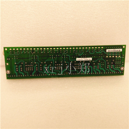
IC670MDL730
IC670MDL730
解决您多处寻找的麻烦和对产品质量的担心等
在价格上我们有很大的优势,欢迎咨询,我们将会给您优致的服务!

GE热销:
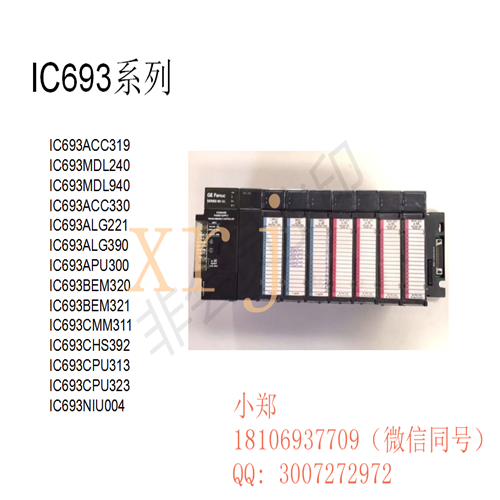
GE697系列
诚信是用不完的资本,信誉是打不倒的招牌
如果您需要,我们能够解决您的缺损部分或交换。
IC697ACC621
IC697ACC624
IC697ACC644
IC697ACC700
IC697ACC701
IC697ACC702
IC697ACC715
IC697ACC720
IC697ACC721
IC697ACC722
IC697ACC723
IC697ACC724
IC697ACC726
IC697ACC727
IC697ACC728
IC697ACC729
IC697ACC730
IC697ACC732
IC697ACC735
IC697ACC744
IC697ACC800
IC697ACC801
IC697ACC802
IC697ACC803
IC697ACC804
IC697ACC805
IC697ACC806
IC697ACC820
IC697ACC821
IC697ACC822
IC697ACC900
IC697ADC701
IC697ADC701RR
IC697ADS701
IC697ALG230
IC697ALG230RR
IC697ALG320
IC697ALG320RR
IC697ALG440
IC697ALG440RR
IC697ALG441
IC697ALG441RR
IC697BEM711
IC697BEM711RR
IC697BEM713
IC697BEM713RR
IC697BEM715RR
IC697BEM721
IC697BEM721RR
IC697BEM731
IC697BEM731RR
IC697BEM733
IC697BEM733RR
IC697BEM741
IC697BEM741RR
IC697BEM761
IC697BEM761RR
IC697BEM763RR
IC697BEM764RR
IC697CBL700
IC697CBL709
IC697CBL803
IC697CBL811
IC697CBL826
IC697CGR772
IC697CGR935
IC697CGR935RR
IC697CHS750
IC697CHS750RR
IC697CHS770
IC697CHS771
IC697CHS782
IC697CHS782RR
IC697CHS783
IC697CHS783RR
IC697CHS790
IC697CHS790RR
IC697CHS790xSV
IC697CHS791
IC697CHS791RR
IC697CMM711
IC697CMM711RR
IC697CMM712
IC697CMM712RR
IC697CMM721
IC697CMM721RR
IC697CMM731RR
IC697CMM741
IC697CMM741RR
IC697CMM742
IC697CMM742RR
IC697CMM798RR
IC697CMM799RR
IC697CPM790
IC697CPM790RR
IC697CPM914RR
IC697CPM915RR
IC697CPM924RR
IC697CPM925RR
IC697CPU731
IC697CPU731RR
IC697CPU732RR
IC697CPU771RR
IC697CPU772RR
IC697CPU780
The software design of the system can be divided into two parts according to the General Division of hardware structure. The whole system runs as shown in figure 2, FPGA AND DSP program run independently, through interrupt signal to complete the real-time interaction of data. The instruction of FPGA TO DSP is to send an Edma request through FPGA. DSP responds the Edma Request, establishes the Edma Channel, and begins to read the pre-processed data from FIFO. When DSP transmits the data to FPGA, it sends an interrupt signal to FPGA, let it read out the compressed image data from Fifo. Mb86s02 video image sensor collects video image information under the control of FPGA. After receiving the command of PC, MB86S02 begins to collect video signal. FPGA, as the core control unit of the system, is not only responsible for collecting video image, and is responsible for the video image information pretreatment and the system unit module between the data interaction. In order to ensure the real-time requirement of the system, the system uses a large capacity off-chip Sdramr to cache the video image information, and the SDRAM controller is implemented by FPGA, after the video image information is buffered by SDRAM, it is first filtered by FPGA to eliminate the noise interference in the image information. In this system, the video information is processed by means of median filter, after filtering the data into the DSP through the FPGA internal Fifo next step compression processing. After power-on, the DSP first loads the bootstrap program and waits for the FPGA to send the request. After receiving the FPGA request, the DSP establishes the Edma Channel to obtain the video data from the FPGA, after storing a full frame, the DSP begins to compress the video image with Jpeg, after the compressed video image information is stored in Fifo, it is written into the USB interface controller's data buffer under the control of FPGA, waiting for the PC's reading request, the USB interface controller writes the data to Port 1 of PDIUSBD12 after receiving the reading request from the PC, so that the PC can read the data next. The whole work flow of the system can be described as follows: After the system is powered on, the DSP is first bootstrapped by Flash, and the BOOTSTRAP program is run, then it is put into the Edma waiting state, and the FPGA initializes and waits for the External Image Acquisition Command, after receiving the command of image collection, the image is collected and preprocessed. The preprocessed image is buffered. After storing a certain amount of data, the FPGA sends the EDMA REQUEST TO DSP through half full signal, once the DSP receives the Edma Request from FPGA, it immediately establishes the Edma Channel, reads the data from Fifo to l2 memory, after storing a frame of image, the DSP starts the image compression, after waiting for an image compression to complete, dSP will send an interrupt signal to FPGA, FPGA receives the interrupt signal and begins to read the compressed image data from Fifo. After reading a frame of data, to determine whether the encoding signal is valid, if valid then according to the same rules for the next frame of image compression, if invalid then inform the DSP en

 客服1
客服1